Preface
The reason I am dedicating a separate blog post to GPU architecture is my realization during the study of GEMM that a concrete understanding of hardware composition and various scheduling mechanisms is essential. Only then can one understand what CUDA can do and what it cannot. I do not intend to explain the full historical evolution; instead, I will briefly introduce the general NVIDIA GPU architectural components required in GEMM, moving from a global perspective to local details. Readers familiar with this topic may skip ahead.
NVIDIA GPU Introduction
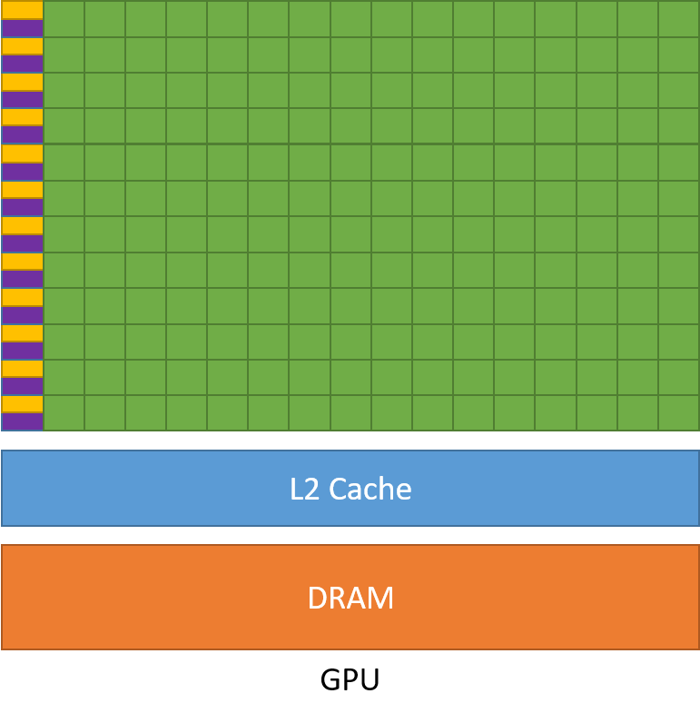
A GPU is essentially hardware designed to run a massive number of threads simultaneously. Threads are the entities being executed, which can be understood as “tasks.” The operator code we write essentially defines the tasks the GPU needs to execute, specifying where to fetch resources and where to perform calculations. The place responsible for executing these threads is called the SMStreaming Multiprocessor, and threads are executed by the cores within the SM. Anyone who has studied Operating Systems knows that caches are introduced to reduce repetitive data access. This applies equally to GPUs, which employ a hierarchical caching strategy where larger capacity implies slower speed. The image above abstracts a rough GPU model: the green parts represent cores for calculation, yellow represents control units, and purple represents the L1 cache. These three together form the aforementioned SM, the actual place where threads are executed. As shown, a GPU contains multiple SMs, and a single SM contains multiple cores for executing threads. Additionally, there are two storage areas at the bottom: the L2 cache and Global Memory (also known as VRAM). Data is first stored in video memory and then sent step-by-step from the bottom into the SM to be utilized by threads. This constitutes the general execution process of a GPU.
Memory Model

As mentioned above, massive numbers of threads are sent to the SM for execution. Their data is passed down level by level, eventually reaching the registers; only data that enters a Register can be used by a thread. Taking data fetching as an example, when a thread requests data from global memory, it first checks if the L1 and L2 caches perform a hit. If both miss, it reads from global memory. During the return process, copies are left in L2 and L1 level by level. In high-performance GEMM operators, we also utilize Shared Memory. The memory access path is Global Memory → L2 → L1 → Shared Memory → Register. In the image on the left, a BLOCK actually represents a collection of threads. This collection is sent into an SM, which executes all threads within that BLOCK. The SM acts like a workbench, containing workers (cores) to execute tasks, containers for storing data (registers unique to each thread and Local MemoryLocal memory is physically stored in global memory; here it is a logical concept within the CUDA programming scope), and Shared Memory accessible by this collection of threads. The diagram also shows Constant Memory and Texture Memory; interested readers can explore these on their own. It is sufficient to understand the rough memory composition and the direction of data flow. To summarize: data required by threads in the SM cores starts from Global Memory, passes through L2 cache, L1 cache, Shared Memory (optional), and finally reaches the Registers for use.
Computational Model
A crucial responsibility of the GPU is computation. Next, I will detail the composition and execution flow of the SM (Streaming Multiprocessor). The evolution of NVIDIA cards from the Tesla model to the current Blackwell model has spanned a long time, but the general framework has actually changed very little. First, let us introduce the concept of the Warp—32As for why it is 32, interested readers can explore NVIDIA's design philosophy on their own adjacent threads in a Block form a Warp. This concept is vital because the SM does not execute threads individually but in groups. This group consists of 32 threads, meaning the minimum unit of execution in an SM is a Warp.
Basic Composition
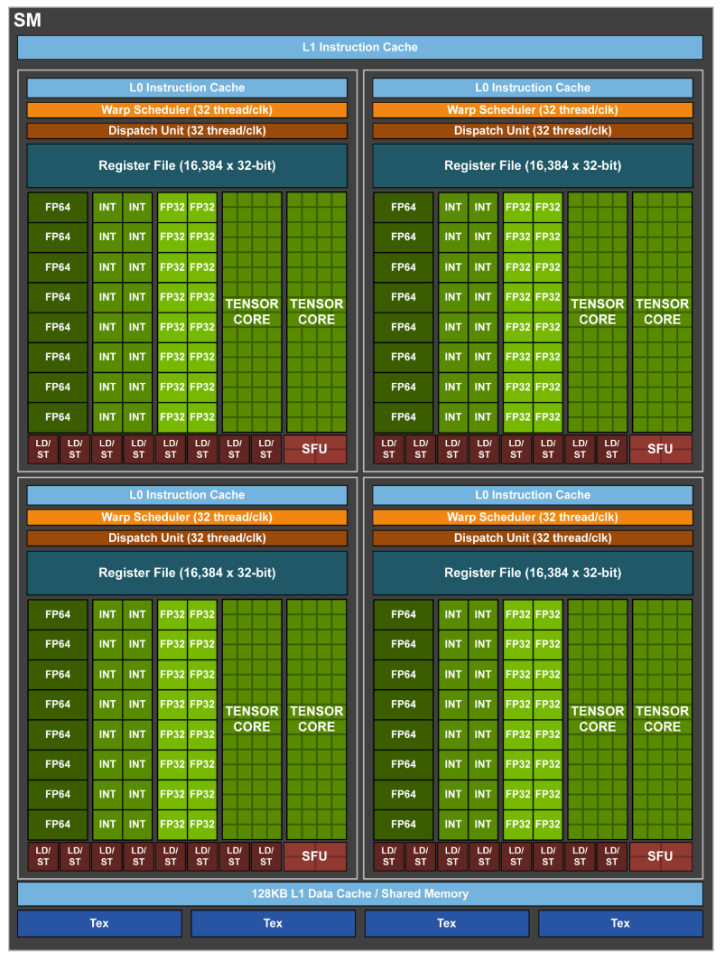
Let us take the Volta architecture as an example. in the Volta architecture, an SM features 4 partitions, each with corresponding cores and storage. When a Block arrives at the SM, the threads inside enter a partition with the Warp as the minimum unit. The green parts in the diagram correspond to cores for differentThis is because the arithmetic logic is completely different; floating-point addition requires normalization, rounding, overflow detection, etc., whereas integer addition only requires addition with carry logic data types. In addition to standard data type operation cores, Tensor Cores appear. These are specifically prepared for deep learning training, which involves massive matrix multiplications. The Tensor Core acts like an API, completing a small matrix multiplication in one go. The remaining cores are called CUDA Cores, where the basic operations we write in kernels are calculated. Each partition in the diagram also possesses an SFU unit designed for special mathematical operations, such as Sin and Cos.
Naturally, having workers is not enough; containers are needed to store data. These containers are the Registers and Shared Memory. Each partition in the SM has a Register File for the private storage of operands and results for each thread. Although the register file of a partition is physically a single block of continuous memory space, logically, the hardware allocates independent register sets for each thread. Threads cannot directly access each other’s registers. However, within the same WarpAdjacent 32 threads are called a Warp, a very important concept, data exchange between threads can be achieved at the register level via shuffle instructions (which will be mentioned in the next blog post). The same concept applies to Shared Memory. Within each SM, SMEM is a continuous addressable memory space, but different partitions have their own independent shared memory regions that are inaccessible to one another. In short, the On-Chip resources available for developers to call are Registers (within a partition) and Shared Memory (within an SM). Readers should note the hierarchical relationship between these two storage spaces. Obviously, storage capacity is limited. If the kernel code written demands a large amount of shared memory or registers, the number of Warps that can run simultaneously in each partition decreases. The ability to hide latency consequently drops. Therefore, in kernel writing, it is always a goal to achieve better performance using fewer resources. In reality, deep operator optimization reveals that everything is a trade-off.
Returning to the process: having resolved who computes and where data is stored, we must address how data arrives. The task of the computation core is to perform mathematical operations, while the “LD / ST” red blocks in the diagram act as units specifically for moving data. Moving data is by no means a simple task; it involves issues such as Transaction CoalescingWhen accessing data, if memory addresses are continuous, multiple operations will be merged into a single transaction to save time, Bank ConflictConflicts occur when accessing SMEM, causing a task that could be completed in one cycle to take more time, and AlignmentIn GEMM, alignment issues mainly appear in vectorized memory access, i.e., fetching four data points at once instead of one, which requires memory alignment. A specialized unit is required to execute this. In short, this unit is solely responsible for data movement, where LD corresponds to LOAD and ST corresponds to STORE.
The final question is: since the roles are clear and everyone knows their duties, who assigns the tasks and tells these roles to start working? That would be the Warp Scheduler and Dispatch Unit in each partition. A Block contains many Warps. The Warp Scheduler decides which of them are ready to be sent to the cores for execution. Once a Warp is designated, the Dispatch Unit issues the corresponding instructions. Since a Warp is mounted to a partition for execution, under the instruction emission of the Dispatch unit, 32 threads execute the same instruction in one Cycle. This is the philosophy of SIMTSingle Instruction Multiple Threads. It is precisely because of the Warp Scheduler and Dispatch Unit that the GPU can achieve efficient latency hiding.
- For example, when two consecutive instructions are a computation instruction and a memory access instruction, the Dispatch Unit can issue them to corresponding execution units (Arithmetic Unit and LD/ST Unit) in different clock cycles. This allows the two types of operations to proceed in parallel, which is the philosophy of ILPInstruction Level Parallelism. If there is a Data DependencyA simple example is when the next instruction requires data calculated by the previous one between these two instructions, the next memory access instruction must wait until the previous computation instruction is completed before it can be issued.
- As another example, when a specific warp stalls due to memory access latency, the Warp Scheduler immediately switches to other executable warps to cover the memory access latency. This is the philosophy of TLPThread Level Parallelism. If there are not enough active warps available for scheduling, the computation units will remain idle, manifesting as low occupancy. We will discuss this in detail later.
Summary
The composition of an SM consists primarily of control units (Scheduler and Dispatcher), cores (divided into computation and memory access), and storage space (Registers and Shared Memory). These components form the flow of modern GPU parallel computing. When optimizing GEMM into deep waters, one must constantly pay attention to Stall issues. It is inevitable to adjust the order of instruction emission to keep the computation cores in a state of maximum load and peak performance.
In fact, in most optimization cases, we always face the bottleneck of data movement, the so-called Memory Wall. The imprecise use of the aforementioned Shared Memory, Registers, and Global Memory can easily cause instruction stalls, resulting in performance degradation.
GPU Memory Access Principles
For the majority of fine-grained GEMM optimization work, one focus is on how to fetch more data within a single time step—maximizing the amount of data moved per transfer—and the other is on the design of overlapping data movement and computation. This text focuses on the former. Regarding the GPU’s multi-level storage, each level has its own access characteristics; how to access memory efficiently is crucial.
Global Memory Access
Global memory corresponds to what we call video memory (VRAM). “Global” means it is visible to all threads and persists throughout the entire lifecycle of the kernel function. Global memory is the lowest layer of the GPU multi-level memory architecture; consequently, it has the largest capacity and the longest latency. Before diving into the principles of global memory access, let us first introduce two concepts: Memory Transaction and Cache Line.
- Memory Transaction: The GPU does not load data individually but in groups. A memory transaction actually defines the minimum unit for GPU data fetching: what is the minimum amount I should fetch each time? For example, if a user wants to fetch one item but the minimum unit is four, the GPU will find the four continuous data items containing the target, fetch them, and discard the remaining three. Careful readers will notice that unreasonable memory access causes waste in transaction utilization.
- Cache Line: A cache line defines the minimum unit of cache modification. When loading data, before formally fetching from global memory, an inquiry is made to L2. If found, it transmits according to the minimum unit; if not found, it loads from global memory, evicts a certain cache line based on a specific strategy, and rewrites it. There is also room for optimization here regarding Cache ThrashingRefers to when a cache line just innocently evicted is needed in the next load, forcing a reload from global memory; thrashing means this process happens frequently; better data loading locality can avoid such problems.
In the NVIDIA Official Documentation
, global memory supports transaction sizes of 32B, 64B, and 128B. Using float (4B) as a reference, these transactions correspond to 8 floats, 8 float2s, and 8 float4s, respectively. We know that the minimum unit of GPU execution is a Warp. When a warp initiates a global memory load request, the GPU determines the number of memory transactions based on the global memory addresses from which the warp fetches data. In reality, to achieve high performance in data fetching, we always aim to acquire the maximum amount of data in the shortest possible time. Consequently, this translates to enabling the GPU to complete data fetching tasks using as few memory transactions as possible. Therefore, we generally aim to use a small number of large transactions for data retrieval. Given the same amount of data, a large number of small transactions generates more memory access instructions, results in poor utilization of memory access bandwidth per transaction, and causes latency because the compiler may not issue these multiple instructions consecutively.
Achieving a minimal number of transactions requires understanding the concept of transaction coalescing. If a warp performs memory access on continuous addresses, transaction coalescing can occur. For instance, when a warp fetches 32 floats, it might generate 32 small 32B transactions in the worst case, or it could generate a single 128B large transactionFor single precision, this corresponds to float4 vectorized memory access.
References
- Intro to GPUs
- Introduction to GPU architecture
- CUDA C++ Programming Guide
- Roberto Di Pietro, Flavio Lombardi, and Antonio Villani. 2016. CUDA Leaks: A Detailed Hack for CUDA and a (Partial) Fix. ACM Trans.
- Evolution of NVIDIA GPU Architecture over the Last Decade: From Fermi to Ampere
- GPU Programming 8: Global Memory 3.1 → Alignment and Coalesced Access